(China (Mainland))

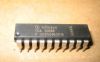
Product Summary
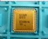
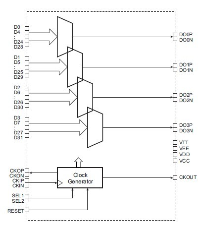
The GD16131-GLP is a 622 Mbit/s MUX/DeMUX Chip Set. It is made as four identical blocks of 8 bit and a clock driver circuit. The 8 bit blocks are implemented as shift registers to obtain the best speed/power ratio of the process technology used. The GD16131-GLP is packaged in 68 pin Multi Layer Ceramic(MLC) packages, yielding excellent highspeed signal accommodation and thermal conditions.
Parametrics
GD16131-GLP absolute maximum ratings: (1)VEE Negative Supply: min=-7 V, max=0 V; (2)VCC Positive Supply: min=0, max=+7 V; (3)VO max ECL Output Voltage: min=VEE -0.5 V, max=0.5 V; (4)VO max TTL Output Voltage: min=-0.5 V, max=VCC +0.5 V; (5)IO max ECL Output Current: max=40 mA; (6)IO max TTL Output Current: max=20 mA; (7)VI max ECL Input Voltage: min=VEE -0.5 V, max=0.5 V; (8)VI max TTL Input Voltage: min=-0.5 V, max=VCC +0.5 V; (9)II max ECL Input Current: min=-1.0 mA, max=1.0 mA; (10)II max TTL Input Current: min=-1.0 mA, max=1.0 mA.
Features
GD16131-GLP features: (1)Quad 8:1 MUX; (2)All high-speed I/O are differential, ECL level; (3)All low-speed I/O are TTL level, outputs drive 10 pF at 78 MHz; (4)Subdivided output clock to data relation selectable in four phases; (5)Dual supply: +5 V, -5.2 V; (6)68 pin MLC flat package; (7)High-speed pins on single side of package for easy PCB routing; (8)Power consumption: 1.3 W typical.
Diagrams
 |
 GD16521 |
Other |
|
Data Sheet |
Negotiable |
|
||||
|
GD16578 |
Other |
|
Data Sheet |
Negotiable |
|
||||